How the CMOSIS buy has beefed up AMS
Riener’s first point was that the acquisition of CMOSIS and its conversion into the CMOS image sensor business line at AMS backs up a goal of becoming a sensor solutions company by broadening AMS’ product range into image sensors. It also gets AMS closer to its goal of more than a billion euros in annual sales, he added.
And it comes at a time when AMS can digest such an acquisition. AMS enjoyed €640 million (about $725 million) in annual sales in 2015; a 36 percent annual increase achieved mostly through organic growth, he said. The acquisition of CMOSIS NV, with about 120 staff, occurred in November 2015. CMOSIS had €60 million of sales in 2015 (about $70 million) with an expectation of growth in 2016 and so promises to add significantly to AMS’ sales in 2016.

The acquisition also helps AMS balance its market diversity, Riener said. AMS has about 70 percent of its sales in the fast-moving consumer market and 30 percent going to the automotive, industrial and medical markets where volumes are unit lower but averaging selling prices (ASPs) are higher and easier to maintain. Meanwhile CMOSIS is more exposed to the high-end professional markets and industrial machine vision.
As well as helping AMS to weather difficult consumer and smartphone markets, CMOSIS can benefit from the AMS sales organization to help it get into new markets – such as automotive and medical – which require lengthy sales and qualification periods, said Riener At the same time AMS can help repurpose CMOSIS technology for consumer applications, he added.
AMS is not one of those companies that says it is necessary to move up the value chain to conduct profitable sensor business (see MEMS sector faces a fight to provide value and Not enough money in MEMS, own the data, says InvenSense CEO).
“We contributed to an IoT work group with McKinsey and the GSA [Global Semiconductor Alliance] with the conclusion that IoT is a growth wave following on from the personal computer and the mobile phone – but it’s not going to change business models. We are good at hardware and maybe software up to the level of drivers, but we are not going to compete with our customers. Sensor nodes and end-to-end systems is not our turf.”
“The key to success is differentiated products, and it helps that we are manufacturer and not an outsourcer,” Riener added.
Indeed not only is AMS a manufacturer but it also offers foundry services and these currently make up about 10 percent of sales revenue. “Foundry increases our own economies of scale in manufacturing, allowing us to reduce pricing, and it is way of keeping antennae up across a broader part of the industry by way of the companies and startups we deal with,” said Riener.
That foundry work could become more significant as AMS brings up its New York fab (AMS to spend $2 billion on New York wafer fab).
“The ground has been broken for Fab C and the shell is going up. Equipment will move in in mid-2017 and we expect to be in production there in the first half of 2018,” said Riener.
In Austria AMS has a manufacturing capacity of 200,000 wafer starts per year (200mm wafer equivalents) and plans to start at Fab C with 50,000 wafer starts per year (also at 200mm wafer size).
Fab C has a planned-for maximum capacity of 400,000 200mm diameter wafer starts per year. There is no definite plan to expand foundry as a percentage of our business, but it may well expand as a consequence of bringing up Fab C Riener said.

But the creation of Fab C and the acquisition of CMOSIS is also a synergistic opportunity for AMS. CMOSIS, founded in 2007, operated as a fabless semiconductor supplier and uses Tower Semiconductor Ltd. and STMicroelectronics NV as its foundries. “It is an opportunity to bring manufacturing in-house,” said Riener.
CMOSIS built its reputation by working at the high performance low volume end of the spectrum and avoiding the high volume and cut-throat world of the smartphone image sensor. Instead it makes high-end, high-resolution sensors with key design wins inside Leica M-model and S-model still cameras and within high-end video cameras – such as those from Black Magic Design – while also pursuing machine vision applications in factory automation and elsewhere. CMOSIS specializes in such things as global shutter sensors and high frame rate sensors as well as extreme complexity.
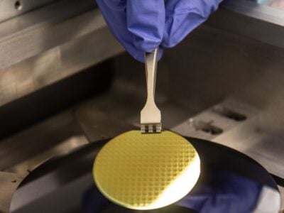
An example of CMOSIS capabilities is the 391-million pixel image sensor on a piece of glass as big as smartphone. It has a resolution of approximately 14,000 by 28,000 pixels. “It is used for a geographical information system. It gives images of the ground with 0.5 centimeter resolution when flown at 2,000 meters,” said Hermans.

To illustrate another extreme Hermans shows a medical sensor; the Naneye. This is a complete camera – including lens, sensor and four-wire interface – in a package that is less than 1mm on a side. “It is designed for disposable endoscopy. We are already in production and expect to ship several hundred thousand units this year,” said Hermans.

“It’s another example of synergy with wafer-level packaging of the lens which is something AMS has in-house,” said Riener. Meanwhile the hunt is on to find other applications that can benefit from a tiny, short depth-of-focus camera. Spectacles and visors for eye-tracking are two applications that have already sprung to mind.
Hermans is also interested in other aspects of image sensor technology based on silicon and CMOS. Two examples are machine vision – where outputs do not need to be in an array format, something that is optimized for humans rather than machines – and hyperspectral imaging.
The IMEC research institute, out of which CMOSIS was created in 2007, is a leader in hyperspectral research (see IMEC hyperspectral image sensor exceeds 140 bands). CMOSIS is a supplier of base image sensor wafers to IMEC but the market needs to develop, Hermans said. “There are possibilities but partly it is about helping applications to develop,” said Hermans.
Some of those applications for both hyperspectral and visible spectrum applications could be on-board drone aircraft. “We are already talking to customers about their applications. Drones are very diverse, from toys to military UAVs [unmanned airborne vehicles]. Obviously at the low-end they will re-use smartphone image sensors for reasons of cost, but at the high-end the requirement is getting close to we are doing in the professional segment,” said Hermans.
Clearly there is an expectation that the CMOS image sensor business line can hit the ground running for AMS but there are also challenges and markets that may take longer than expected to develop. Being part of AMS gives more time to develop applications in areas like medical automotive image sensing.
Related links and articles:
News articles:
MEMS sector faces a fight to provide value
Not enough money in MEMS, own the data, says InvenSense CEO
AMS to spend $2 billion on New York wafer fab
IMEC hyperspectral image sensor exceeds 140 bands
 If you enjoyed this article, you will like the following ones: don't miss them by subscribing to :