Open design for large scale quantum computer
An international team of researchers have developed an open design for a trapped ion quantum computer.
The international collaboration. led by the University of Sussex in the UK, includes scientists from Google US, Aarhus University in Denmark, RIKEN research institute in Japan and Siegen University in Germany. They developed a simpler modular design that used electric fields to transfer ions without having to align laser beams, allowing for a scalable architecture.
Quantum computing on a small scale, using trapped ions, is carried out by aligning individual laser beams onto individual ions, with each ion forming a quantum bit. A large scale machine with billions of quantum bits needs billions of precisely aligned lasers, making it impractical.
‘For many years, people said that it was completely impossible to construct an actual quantum computer’ said Professor Winfried Hensinger, Director of the Sussex Centre for Quantum Technologies and research lead for the project. He has been working on trapped ion quantum technology for over a decade.
‘With our work we have not only shown that it can be done but we’ve delivered a nuts and bolts construction plan to build an actual large-scale machine. And now we’re building a prototype based on this design,” he said.
Related trapped ion quantum computer articles
- Quantum computing startup bets on trapped ions
- Infineon steps up move to quantum
- CEO Interview: Building a quantum computing leader in Europe
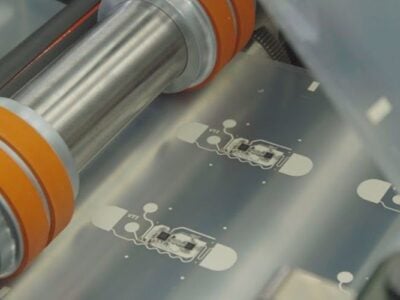
The modules control all operations as stand-alone units and are constructed using silicon microfabrication techniques possible with current 5nm technology. The modules use long-wavelength (microwave) trapped ion quantum gates, with the quantum bits transmitted between individual modules using electric fields. This is 100,000 times faster than using an optical fibre link, says the researchers and allows many modules to be connected to construct a large-scale device.
A high error–threshold surface error correction code can be implemented in the proposed architecture to execute fault-tolerant operations, and the design is suitable for other trapped ion quantum computer architectures, such as schemes using photonic interconnects.
Quantum computer design
Each module uses microfabricated ion trap X-junction arrays where two or more ions are trapped. These have three different zones, with a microwave-based gate zone, a state readout zone, and a loading zone. Once an ion is trapped in the loading zone, high-fidelity ion shuttling operations transfer the ion to the gate zone. There, ions can be individually addressed using locally adjustable magnetic fields and entangled using static magnetic field gradients in conjunction with global microwave and rf fields.
When the state of the qubit needs to be detected, the ion is transferred to the readout zone, where global laser fields and on-chip photo detectors are used for state readout. A second ion species is used to sympathetically cool the qubit ion without affecting its internal states.
All coherent quantum operations are performed and controlled by on-chip electronics, relying only on global microwave and rf fields. In this architecture, laser light is only required for state preparation and detection, photoionization, and sympathetic cooling. This means the laser beams can have much less stringent requirements than those used for quantum gate realization. The laser beams do not need to have high intensity, and do not need to be phase-stable.
5nm process technology
The X-junction structures occupy an area of 2.5 × 2.5 mm2 and can be fabricated in large numbers on a silicon wafer to form the scalable quantum computer module. A total of 1296 individual X-junctions can be monolithically fabricated onto a 90 × 90–mm2 silicon wafer piece, compatible with standard 150-mm wafer sizes.
However, the challenge is the power supply. If all of these X-junctions are electrically connected together, the capacitance and power dissipation will become too large to be driven with a standard helical resonator of high-quality factor. As a result, the vacuum system for the trapped ions and the cooling system restrict the size of the modules.
The team used the Advanced Design System software tool from Keysight Technologies to simulate 6 × 6 junctions connected together in an electrical submodule. This keeps the capacitance below 80 pF, and a quality factor of Q > 200 is achievable using a compact helical resonator of 15 mm in diameter.
An additional requirement to achieve a high-quality factor is to use a substrate with low rf loss, typically with a bulk resistivity of 50 kΩ·cm. Compact resonators are placed inside the system underneath the module and connected with shielded cables to the electrical submodules. All resonators are attached to the same frequency source, and the resonant circuits are tuned into resonance with the frequency source using variable capacitors.
The close proximity of the electrical sections will lead to capacitive coupling between the resonators and, as a result, lead to phase matching of the resonators and neighbouring rf electrodes. Careful design of the connection paths on the ion chips is used to avoid non-negligible phase differences between relevant rf electrodes.
Each electrical submodule features 1224 static voltage electrodes and 108 individual local gradient current wires. The required static voltages and currents are supplied by DACs inside the vacuum system, fabricated on separate silicon substrates, which are attached to the ion trap substrate using TSV and wafer-stacking technology.
Stacked readout electronics
Each wafer layer features four DACs with 160 analog outputs in total (the AD5370 has sufficient outputs and was used as an example, but a modified version will be required that operates at higher update rates) and, combined with the required TSV and RC filters, occupies an area of no more than 15 × 15 mm2. Generating enough analog outputs requires a total of nine wafer layers that will be stacked together. An additional layer is used to house an electronic control unit, which controls the in-vacuum DACs and detection system.
The embedded copper wires generating the magnetic field gradients are routed in such a way that only four high-current connections are required per module but these are passing large currents of 10 A through wires with a small cross section (~30 × 60 μm2). This makes it essential that the resultant heat is efficiently distributed and transported away from the modules. In addition, the power dissipated by the ion trap structure and the in-vacuum electronics needs to also be transported away from the modules. Melting of the wire structures can be avoided by cooling the silicon substrates to below 100 K.
The team propose using a liquid nitrogen microchannel cooler integrated into the back wafer of the modules to efficiently remove the heat from the modules. Deep trenches are etched into the backside of the last wafer, forming channels through which liquid nitrogen is passed. The channels are covered using an additional silicon wafer. Fabricating the entire module including the liquid cooler out of silicon prevents additional stress and wafer bow arising from different thermal expansion coefficients.
Each of these modules with the 6 x 6 sub-modules can work as a stand-alone small-scale quantum processer module with 1296 X-junctions.
The research is part of the UK Government’s National Quantum Technology Programme.
“The availability of a universal quantum computer may have a fundamental impact on society as a whole. Without doubt it is still challenging to build a large-scale machine, but now is the time to translate academic excellence into actual application, building on the UK’s strengths in the technology,” said Winfried. ‘We are very excited to work with industry and government to make this happen.”
Related articles
- Europe’s quantum tech on show at MWC
- Merger creates quantum computing giant
- Quantum project for digital twins
- UK opens up £6m quantum technology competition
Other articles on eeNews Europe
- Tackling the challenges of RISC-V
- Espressif moves exclusively to RISC-V
- European project for ‘brain-like’ AI
- Video shows world record speed for autonomous car
- High speed MRAM memory for FPGAs
 If you enjoyed this article, you will like the following ones: don't miss them by subscribing to :