Closing the Memory Gap: Can Advanced Fab and Packaging Finally Realize In-Memory Processing?
Abstract:
Rapid advances in processing, led by domain-specific silicon and better use of resources, are placing pressure on memory systems to provide enough data to keep these engines running at top speed. Among the ideas receiving increased attention are moving processing closer to the data, and applying new architectures to eliminate bottlenecks in memory and networks. A number of technical challenges must be addressed before the industry can bring these solutions to market.
Introduction: Computing Bottlenecks are a Moving Target
Processing, memory, storage, and networking are the four pillars of enterprise-class computing. Ideally, these critical subsystems should be in balance for optimum performance and efficiency. Of course, the reality is never that simple; each of these leverages different technologies that follow their own innovation and development trajectories, with the result that improvements in one subsystem inevitably shifts the balance of a system, leaving others needing to catch up.
Today, CPUs and GPUs have become so fast that these processors often must wait for data from memory before they can continue working. Recent advances in processing have exacerbated the decades-old “Processor-Memory Gap,” with modern systems often left struggling to move data from storage and memory to the processors, across interfaces that have limited bandwidth.
Particularly challenging are workloads that involve filtering large quantities of data to look for a small number of items – akin to finding a “needle in a haystack.” These include certain types of database operations like search, which are computationally untaxing but involve the movement of vast amounts of data over already stressed interconnections. Moving so much data from memory and storage to the processor, only to realize that you don’t need most of it, wastes considerable time and energy. In some cases, the amount of energy spent moving data to the processor can be about 100 times larger than the amount of energy spent doing simple operations on the data.
Next: Big data demand
Given that demand for higher-performance search, analytics, and data processing are accelerating in areas like Big Data analytics and AI solutions are needed to dramatically improve the speed at which data can be moved to the processor from memory, storage, and networks, and to reduce power consumption in the process. Without these solutions, future processing capabilities will not be able to achieve their full potential.
The gap between processor performance and the other subsystems has been growing for several decades. Solutions put forward in the past to address this gap have included various processor-in-memory (PIM) strategies, such as computational RAM or Intelligent RAM (IRAM). Each of these approaches bring their own opportunities but also face some difficult implementation challenges. With the semiconductor industry energized by advances in AI and Big Data, the industry is re-examining some of these approaches to address the need for faster, more power-efficient data movement. In particular, the semiconductor industry has made critical advances in process technology, packaging, and 3D die-stacking that can potentially improve data movement. The memory industry has made similar advances, with advanced packaging and 3D die stacking helping to enable the current generation of high-bandwidth memory (HBM) memory devices.
It’s worth mentioning that the familiar cache memory (which resides on the processor) is a tried and tested solution to accelerating CPU performance by loading needed data into on-chip memory close to the processor. Simply increasing the cache size could allow the CPU to tackle larger data-intensive tasks more quickly. However, caches consume a large quantity of silicon area and power, so larger caches aren’t always the best answer. Furthermore, as caches get larger and faster, they place increasing demands on memory, storage, and networks to supply them with growing amounts of data more quickly. A more cost-effective and energy-efficient solution is required.
Next: iRAM
Processing in Memory
IRAM calls for a small processing element to be integrated in the DRAM chip, which is optimised to perform basic computations and filtering before passing the data to the main CPU. This could drastically reduce the quantity of data being passed back and forth between the memory and the CPU during workloads such as database searches, and hence significantly increase performance while also saving power.
However, there are both performance and cost challenges with using a processor-in-memory approach. DRAM processes are optimized for building small memory cells with minimal charge leakage to retain data. The best silicon processes for fabricating CPUs and GPUs, on the other hand, are designed for fast transistor switching to improve performance. In addition, in part due to the fast transistor switching, processors dissipate significantly greater power than DRAM cells, which can challenge the thermal performance of traditional low-cost memory packages. DRAMs have a harder time retaining data as temperatures increase, which can necessitate higher refresh rates that reduce the bandwidth they can provide. For these reasons, combining both memory and processing on the same die, in close proximity, is particularly challenging. There are also associated cost challenges, because the testing of combined processor/DRAM dies is more time-consuming as well.
Upmem has recently tackled some of these issues with its novel Processor in Memory DRAM (PIM-DRAM) chips by creating a simplified processing element that can be fabricated in two or three metal layers and hence can be manufactured in a small die area on a standard 20nm-class DRAM process. One of these Data Processing Units (DPU) is connected to each 64MB of DRAM, using an interface that has an equivalent 1GB/s bandwidth, and supports a simplified instruction set that has the advantage of being easy to program (see Processor-in-memory DRAM benchmarked on Xeon server).
An 8Gbyte DIMM built with 16 of these PIM-DRAM chips would contain 128 DPUs. Simulations have shown that genomics pattern matching could run as much as 25 times faster, while database searches could be 14 to 18 times faster.
Next: 3D stacking
3D Stacking Memory and Processor Dies
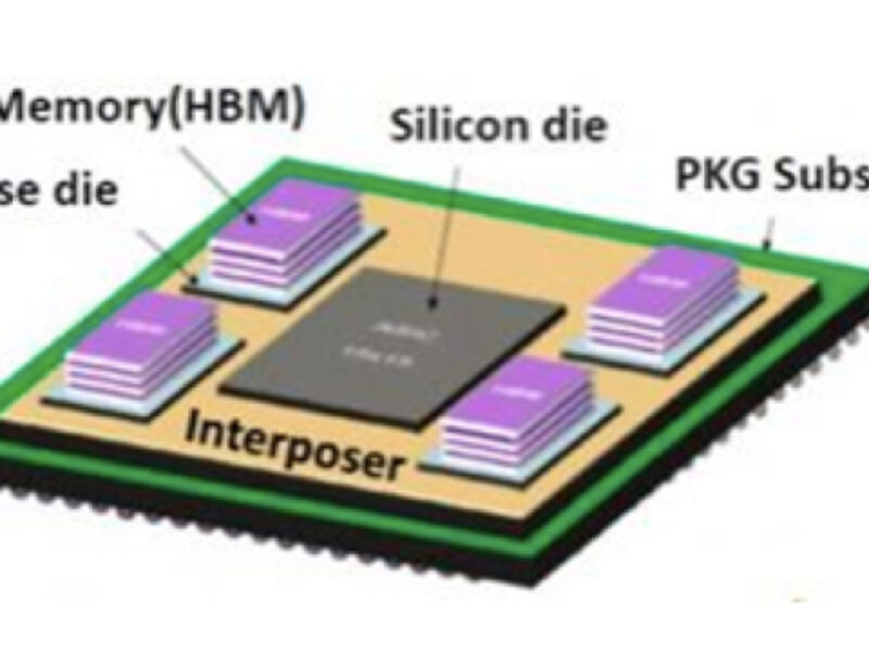
As an alternative to the processor-in-memory approaches that push the processing onto the same die as the DRAM cells, a 3D stacked device can be created that combines a dedicated processor die and DRAM die that are interconnected with through-silicon vias (TSV). This would allow the processor and memory to be manufactured using the most appropriate process technology for each, and then joined together to minimize the distance that data travels. TSVs, which are a necessary tool for die stacking, have been in use for several years in HBM memory devices as shown in figure 1.

Figure 1. HBM memory uses stacked die interconnected using TSVs. HBM memories are connected to the SoC through an interposer to achieve a wide, high-bandwidth memory interface.
By taking the next step and combining processor and memory into a single stack, there is the potential to dramatically increase both the speed at which data can be transferred to the processor, as well as the energy-efficiency, while also avoiding the challenges of manufacturing processors in DRAM processes. The potential to place processor cores and associated DRAM blocks on different die but at corresponding locations on their respective dies allows for short and direct connections between the two, avoiding conventional interconnect issues associated with discrete (unstacked) chips such as larger bondwires, leadframe, and I/O pads and pins that also sap energy and introduce delays.
3D stacking combines the performance gains of in-memory processing with the advantages of die separation. In addition to being able to optimize the processor die for high-speed switching while designing the DRAM for low cost and best charge retention, another advantage is that all dies can be individually tested so that only known-good processors and DRAMs are paired, thereby improving manufacturing yield.
One of the biggest challenges with 3D stacking is thermal management, in this case ensuring the heat dissipated by the processor does not impact the charge retention in the DRAM chip. Although the shorter distance between memory and processor should help reduce power dissipation, the potential to increase processor performance because of better memory performance will mean that power may well increase, making it a challenge for the foreseeable future. Further research and development is needed for addressing the need for lower power, better thermal conduction, and better cooling methods.
Conclusion
For the past 30 years, Rambus has been developing innovations to improve the movement of data between processors and memory in order to address the Processor-Memory Gap. In the past, the semiconductor industry has relied on Moore’s Law and Dennard Scaling to deliver more transistors and lower power, respectively, enabling the industry to deliver tremendous gains in performance with each new generation. But these gains are either slowing (Moore’s Law) or have stopped (Dennard Scaling), just at a time when the industry needs them the most. Our industry has responded by re-examining how chips are designed, with breakthrough advances coming from domain-specific silicon. Additional research and development is taking place to develop the next enablers of performance and power-efficiency gains, and has re-ignited interest in Processing-in-Memory as well as 3D stacking. Some barriers still exist for both, but the potential gains make them intriguing and active areas of research in the industry.
Related links and articles:
News articles:
Rambus, GigaDevice form ReRAM joint venture
Rambus to buy Inphi memory interconnect business
Weebit, Technion collaborate on processing-in-memory
Processing-in-Memory architecture takes embedded AI to 8.8 TOPS/W
Processor-in-memory DRAM benchmarked on Xeon server
 If you enjoyed this article, you will like the following ones: don't miss them by subscribing to :