First carbon nanotube NRAM products due in 2020, says Nantero
Bill Gervasi, principal systems architect at Nantero (Woburn, Mass.), said the company is also busy helping to install its technology in a memory production line of a licensee. Gervasi said he expects high capacity memories to come out of that facility in 2021.
The enduring interest in NRAM – despite a protracted coming to market – is because the technology is compact, offers non-volatility with the speed of DRAM, with potential for scalability beyond DRAM and superior endurance to flash. It is closer to a universal memory than almost all of the rich field of emerging memory technologies – PCM, MRAM, ReRAM. Whereas those memory technologies are generally pitched to replace flash memory, NRAM could theoretically find slots both as a DRAM replacement and as a storage memory replacing flash. NRAM has been thwarted to date largely by the economics of replacing incumbent technologies that are low cost due to their established scale of manufacturing
Now the first products are expected from Nantero’s licensee Fujitsu Semiconductor in partnership with USJC – a subsidiary of foundry United Microelectronics Corp. Fujitsu took out its license in 2016 and has touted Nano-RAM (NRAM) as suitable follow-on technology for its ferroelectric RAM products, which it uses both discretely and embedded alongside microcontrollers.
Gervasi said: “The Fujitsu parts are on-track for mass production this year.” He said that he understood one of the products would be a stand-alone memory and another would be a logic device with embedded NRAM.
Next: The mat of CNTs
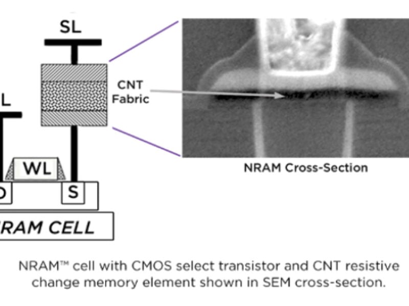
The mat of CNTs
The technology is based on a slurry of randomly organized carbon nanotubes arranged in a thin layer between cross-point electrodes. When a voltage is applied the CNTs are drawn together and increased numbers of contact points reduce the resistance path between the electrodes. The connection is maintained by Van der Waals forces at the atomic level. To reset the memory cell, a voltage pulse causes thermal vibration to break those connections.
The resulting memory offers switching speeds of the order of 20 picoseconds at low energy together with a practical write speed of 5ns with endurance of the order of 10^11 cycles. This holds out the prospect that CNT-based NRAM could be superior to competitor technologies such as ReRAM and phase-change memory and scale better in physical geometry to become a universal memory to replace both DRAM and NAND flash memory.
One relatively recent sophistication is the addition of a layer of aligned CNTs above the randomly organized “mat” of switchable CNTs. These serve to protect the lower layer of switching nanotubes from metal migration from the sputtered metal above.
Gervasi did not say exactly how CNTs perform against filament formation after many switching cycles. “We don’t use a metal like silver that would promote filament formation. We do have a titanium-nitride barrier layer between the copper electrode and the top of the CNT cell. It could equally well be aluminum electrode.”
Nantero was founded in 2001 and its path has been difficult and many times the company has claimed to be close to production. Nonetheless it has gradually acquired backers and licensees. Gervasi said that the company is just closing an H round of equity financing that takes the company above $140 million in terms of money raised.
Long-time investors include Dell, Cisco, Kingston Technologies and Schlumberger. Another is CFT Capital a Chinese venture capital firm incorporated by SMIC, mainland China’s most advanced semiconductor foundry. More recently the company has added Globespan Capital, CRV, Draper Fisher Jurvetson and Stata Venture Partners.
Next: Stacking and MLCs
Stacking and MLCs
However, to compete at the leading-edge with DRAM and flash Nantero may have to add 3D stacking, fortunately something that the technology is readily capable of accommodating. “We already do stacking,” said Gervasi indicating that unnamed memory partner is working on a 4-layer 16Gbit device on a process at between 22nm and 18nm.
Gervasi said that Nantero also knows how to do multi-level cell at least up to two or three bits per cell. “In terms of voltage we are 30x between set and reset. It is a linear relationship but we are stochastic,” he added. That means precise levels would vary from cell to cell making it hard to go further without calibrating each memory cell. Gervasi said it would be possible to go further with a form of iterative cell writing. “Sequential writing costs time but with 5ns write speed that is something we have,” Gervasi said.
Gervasi points out that economics and market entry are at least as important as the technology. The extremely low cost of NAND flash makes it a difficult market to address initially he said. For DRAM however Moore’s Law has stalled.
“Three years ago the end users weren’t pushing [for higher capacity DRAMs]. Then artificial intelligence and machine learning erupted in the cloud. There is a lot of re-architecting going with demand for high capacity memories and non-volatility.
Related links and articles:
News articles:
Fujitsu is licensee of Nantero’s carbon-nanotube RAM
CEO interview: Nantero’s Schmergel says NRAM production is close
Second Chinese chipmaker signs up for Weebit’s ReRAM
This 8Mbit ReRAM from Fujitsu doubles capacity
Embedded MRAM available on 22nm FDSOI
China’s XTX adopts Weebit’s ReRAM
Carbon nanotube processor breakthrough made at MIT
 If you enjoyed this article, you will like the following ones: don't miss them by subscribing to :