Forum goes back to the future in Antwerp
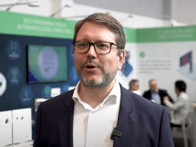
The forum takes place May 23 and 24 at the Flanders Meeting and Convention Center in the centre of Antwerp. Luc Van den hove, CEO of IMEC, discussed some of the themes coming up at the event and how developments and areas of interest are changing at the research institute.

“The theme of this year’s IMEC Technology Forum is making the impossible possible. With technology, we can create phenomenal applications and connecting various technologies can lead to unexpected opportunities. Progress continues with traditional scaling but is also diverging in many directions. In my talk, I will emphasize opportunities arising from the many and various links between biological knowledge and semiconductor knowledge.”
“Semiconductor technology and Moore’s Law has enabled DNA sequencing to be done faster than ever before. Meanwhile neuromorphic computing, which is biologically inspired, and artificial intelligence is reducing power consumption and increasingly being deployed at the edge of the system,” he said.
Van den hove then gave an example of how semiconductor and biological knowledge and expertise can move back and forth – like a wave in a bath – reinvigorating development at each end with each surge of the water. Having enabled DNA sequencing, computer memory could in future be based on biological material such as DNA. The method is to use the base-pair molecules A-T and C-G, with combinations of ATCG laid down to represent and store binary data.
“Using such a system we can store a petabyte of data – 10^6 Gbytes – in one gram of DNA material. We need to learn how to read and write such data but the principles of this are being explored in the DNA sequencing domain,” said Van den hove.
Next: Joining the dots
The rise of life science interests at IMEC dates back 15 years or so and roughly coincides with a broadening of corporate interest in applying semiconductors to those things of fundamental interest to human beings; health, mobility, environmental comfort, entertainment, whereas prior to that time semiconductor ICs and their development were more of professional and specialist concern.
“It was an important transition. Twenty to thirty years ago semiconductor research enabled the ICT [information and communication technology] revolution. But now semiconductor technology can impact so many other grand challenges. The technology has a broad impact and we at IMEC realized we need to put technology in a social context.
It is notable that at the ITF will include presentations from: Thomas Müller, executive vice president of electronics development at Audi on mobility in 2025; Jay Flatley, executive chairman of Illumina on DNA sequencing; and Matthew Mattina, senior director of machine learning and AI research at ARM.
Van den hove said that in the past there had been relatively few people interested in deep technology and it had often been presented in a negative context. “For example the possibility that Industry 4.0 would involve a loss of jobs. So it is very important to let people know about the positive things we can do; in health, in mobility and elsewhere. We want to create enthusiasm, fascination and passion to ensure we have the students, engineers and executives to take us forward in these directions.”
But with the growing ubiquity of electronics there is also an issue of whether various developments are sustainable on a global scale. “There are issues of the scalability of our technology in terms of energy consumption and materials availability in our roadmaps. That is why there is always a drive towards energy reduction and we take into account materials concerns.” But van den hove acknowledged there is more to be done to alleviate problems.
Next: Memory bottleneck
One of the big pressure points in present day electronics is the so-called memory bottleneck, van den Hove said. With ever increasing amounts of data being captured by image and other sensors, performance is increasingly limited by the time and energy cost of moving data to and from processors. So, is the solution a change in memory device or in computer architecture?
“The answer is a combination of both,” said Van den hove. “Scaling of some conventional memories continues – such as 3D NAND flash memory; there are also different innovations in memories, but also we are looking at how to compute at the edge so there is less need to move data to the cloud. We are also being helped by new computer concepts such as neuromorphic computing and cryo-temperature storage.”
One of the ideas that comes out of neuromorphic computing is in-memory computing. “We gave a glimpse of this at ITF last year and we will give an update this year,” Van den hove said.
There are at least two major strands of development in artificial intelligence hardware. One is the relatively near-term development of machine learning hardware based on the implementation and acceleration of simplified artificial neural networks.
While that can provide exciting possibilities, it does tend to depend on fairly conventional logic architectures and asymmetric training and inference procedures. The training can be based on very large data sets which can be good for accuracy but this is by its nature, energy consumptive, even when done in the cloud. More advanced neuromorphic architectures seek to follow the biological model of the brain more closely, with stricter models of the analog behaviour of synapses and axons and reinforcing and inhibiting impulses and with capability for independent, self-learning. While such systems could learn to construct their environment, rather like a baby learns, the electronic domain has the advantage of being able to share that learning efficiently, creating swarm intelligence.
“The impression I have is that both are evolving quickly and it depends on the application. We have fast pattern recognition algorithms but also autonomous system self-learning is going to be extremely important, for example is things like autonomous driving. It tends to impact in-memory implementation. In the first case there may be a tendency to use STT-MRAM [Spin-Transfer Torque Magnetic Random Access Memory] while in the second case with self-learning researchers are tending to look more to the analog behavior in Resistive RAM.”
There is a break-out session on machine learning on the first day of the ITF and Nigel Toon, CEO of Graphcore Ltd., is due to discuss his company’s Intelligence Processing Unit (IPU), which has been designed to accelerate machine learning and AI applications.
Next: Top up on transistors
One thing that has changed in the year since the last ITF in Antwerp is that the industry has, at last, entered the era of extreme ultraviolet (EUV) lithography, something that IMEC has helped pioneer for nearly two decades. “For 7nm and 5nm it is clear that EUV lithography will be the main innovation. But to get below 5nm, to achieve the density improvement there is now a strong focus on the back end,” said van den Hove. “With things like [FinFET] track reduction on the design side, the very aggressive scaling of gate pitch is a bit relieved.
The next question is: which of the various proposed followers to the FinFET will make it to mainstream production and when? “The FinFET extends certainly to 5nm and maybe below. The challenge for FinFET is the short channel effects and really that needs a gate-all-around [GAA] structure. However, we now think 3nm is less likely to need GAA because metal pitch is scaling more aggressively than gate pitch.”
The ultimate design scaling is when there is just one fin per transistor and this is the moment when multiple nanowires or nanosheets will come in, Van den hove said. That is an option for 3nm and IMEC presented a paper on that at IEDM 2017. The nanosheet is basically a flattened or widened version of the nanowire with the ability to carry more current than a nanowire, said Van den hove. The next extension of that development is the complementary FET or CFET in which a single fin may carry p- and n-type the nanowires/nanosheets to create a compact support for CMOS logic.
And in terms of materials van den Hove said things are likely to remain with the status quo at least for logic processes. “Silicon-germanium is in use now. Inserting III-V materials is so much more difficult at least for logic. We are pursuing this kind of model but for more RF performance,” he said.
The ITF will cover just about everything from the deepest technology roadmaps up to varied applications in smart cities and IoT. This year there is also a break out session on the business side of scaling technology from an initial experimental setting into a global business. In short the ITF will be discussing both the future of nanotechnology and, because of technology’s impact, the future of society.
Related links and articles:
News articles:
Evolving IMEC prepares a welcome in the City of Things
Western Digital broadens IMEC collaboration
IMEC, Cadence tape-out first 3nm test chip
Graphcore’s two-chip ‘Colossus’ close to launch
Machine learning interview with Jem Davies of ARM
 If you enjoyed this article, you will like the following ones: don't miss them by subscribing to :
eeNews on Google News


