Nanoscale MEMS Resonator Structure Yields Controllable MHz-Range Filter, Isolator
As electronic devices shrink, there’s an increasing need for on-chip high-performance functions such as unidirectional waveguides (isolators), filters, and delay lines, especially those with key parameters that can be controlled on chip. A team of researchers from ZTH Zurich and Caltech is using silicon-nitride (SiN) nanomembranes that operate at high frequencies (10-20 MHz) as conduits for phonons, the acoustic-like waves passing through a solid or liquid material to build such devices (a situation very roughly analogous to surface-acoustic-wave, or SAW, devices). The nanoelectromechanical metamaterials (NEMM) include the voltage-controlled frequency tuning of the individual resonators.
They fabricated and tested high-frequency “topological” insulators with six lattice sites in a unit cell. The nanoelectromechanical lattice (NEML) design has periodically etched holes of 500 nm diameter in an extended honeycomb lattice, and insulating Si-rich silicon-nitride (SiNx) membranes (average thickness of ~79 nm) that form a phononic crystal with periodic, curved boundaries (see figure 1).

The neighbouring membranes are overlapped to create mechanical coupling. By changing the distance between etch holes, the researchers were able to control the amount of lattice coupling. Their work has been theoretical, beginning with a discrete mass-spring model and the many forces on each element (see figure 2).

for analytical calculation of frequency dispersion.
At the top of (a) is the false-color scanning electron
microscope image showing three unit cells with the
deposited electrodes; at the bottom is a schematic
diagram of the mass-spring systems used to solve
the dynamic model. A close-up view of a half-unit cell
(b) shows the two rotational springs connected by a rigid
bar, and the elastic foundation, showing all relevant
parameters and degrees of freedom. (Source: Caltech)
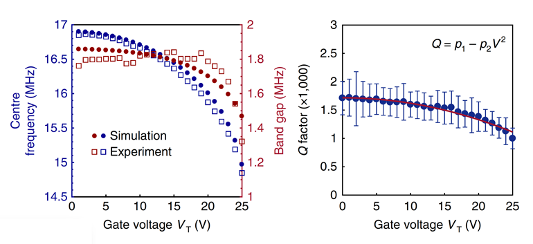
They then proceeded to in-depth, deep-dive physics analysis of the lattice’s electromechanical and related properties, as well as its responses. Finally, they went beyond the theory and its postulated performance by fabricating and evaluating several devices. By applying a dc gate voltage VT to create a voltage-dependent electric field, they were able to significantly shift the frequency bands of the device (see figures 3 and 4).
It’s desirable that a physical channel being used as a waveguide be both stable and defect-free for reliable, consistent performance. However, they noted that energy transport in high-frequency mechanical systems, such as these microscale phononic devices, is particularly sensitive to defects and sharp turns because of backscattering and losses.

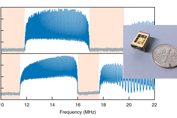
The upper panel shows the response of the device
without electrodes, while the lower panel is with
electrodes; the shaded area indicates the frequency
stop bands. (Source: Caltech).
Since actual devices aren’t perfect, they also investigated the influence of possible fabrication errors that happen during the deposition process. In this case, the non-uniformity in the film thickness causes disorder in the mass matrix parameters used in the many equations of the dynamics.
Another interesting feature of the design is its robustness with respect to waveguide imperfections such as sharp corners. To study this, they also fabricated a zig-zag waveguide with two sharp corners of 60⁰. Their test results showed that the energy transport had negligible backscattering from these corners.
The researchers maintain they have tangibly demonstrated that nanoelectromechanical metamaterials can create on-chip acoustic devices that function as stable yet controllable ultrasound-based, RF signal-processing elements. Their extremely detailed published papers provide full analysis of the molecular and lattice physics, the fabrication process for their devices, their simulation results, and actual measured data. Support for the research was provided by the National Science Foundation, the Binnig and Rohrer Nanotechnology Center at IBM Research-Zurich, and the Kavli Nanoscience Institute at Caltech.
This article first appeared on Electronic Design – www.electronicdesign.com
 If you enjoyed this article, you will like the following ones: don't miss them by subscribing to :