Report: TSMC plans Japan R&D center ahead of packaging facility
The R&D facility will develop advanced semiconductor packaging and testing technology and would be complementary to a volume packaging production line that TSMC is also considering to build in Japan as part of a joint venture (see Report: TSMC, Japan to share cost of Tokyo chip facility).
Japan had been seeking domestic involvement from TSMC in 2020 (see Now Japan wants a domestic TSMC fab) as a response to increasing geopolitical tension around the world, and US moves to draw chip manufacturers on-shore (see TSMC dragged to the altar of US manufacturing).
There were plans for a semiconductor R&D facility as a pre-cursor activity to building a leading-edge wafer fab that could provide Japan’s fabless chip companies of some sort of security of supply. However, TSMC has reportedly persuaded Japan to partner with it on chip packaging.
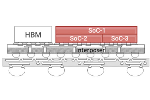
A revolution in chip packaging based on the use of multiple “chiplets” on silicon interposer substrates is expected to have a dramatic effect on chip and system design in the coming years. Japan is a good source of materials for semiconductor manufacturing and for packaging and TSMC has partnered with many of these equipment and materials companies in Taiwan.
TSMC could announce the packaging R&D plans in the next few days, Nikkei said.
Related links and articles:
News articles:
Report: TSMC, Japan to share cost of Tokyo chip facility
TSMC picks Arizona for 5nm wafer fab
Now Japan wants a domestic TSMC fab
TSMC dragged to the altar of US manufacturing
Chiplet-savvy TSMC to build $10 billion assembly and test plant
 If you enjoyed this article, you will like the following ones: don't miss them by subscribing to :