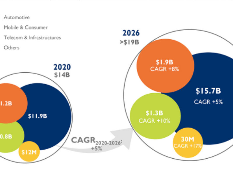
System-in-package market showing 5% CAGR
The market covers multi-die integration for mobile handsets and die-to-die chiplet integration for high performance, said Vaibhav Trivedi, an analyst at Yole Développement.
The strongest growth is in the high-end system-in-package where it is expected to grow at 9 percent CAGR from 2020 to 2026. The low-end RF SiP market, found in mobile phones, is expected to grow at a CAGR of 5 percent over the same period.
System-in-Package technologies include: flip-chip and wire bond-based packaging; fan-out based multi-die form factors and embedded die formats.
The flip-chip and wire-bond based part of the SiP market is expected to reach US$17 billion in 2026 with 5 percent. Embedded die SiP is expected to reach US$189 million in 2026 at a 25 percent CAGR. The fan-out SiP market is expected to reach US$1.6 billion in 2026 at a CAGR of 6 percent.
The SiP remains a crucial platform as it allows the OEM customer to integrate one or more functionalities onto a substrate-based package instead of integrating it as a discreet component on the printed circuit board.
With the rise volumes of SiP components many device wafers are being provided with flip-chip bumping or ball-drop processes as these can be deployed in SiP packages instead of using wire-bonding to attach die.

Key parameters for the System-in-package technology roadmap 2017 to 2025. Source: Yole Developpement.
“In terms of technology and a roadmap, the SiP platform continues to push the boundary in the race to produce denser, thinner, and smaller form factors. These new process technologies include double-side moulding technologies that eliminate the underfill operation from the bottom die resulting in an improved cost structure and manufacturing efficiencies,” said Favier Shoo, an analyst at Yole, in a statement.
In terms of package height, OSATs are expected to push for 0.6mm total package height for SiP devices in the coming years. IDMs, such as Intel and Samsung, are driving hybrid die-to-die interconnect-stacked-packaging, such as Intel’s Foveros architecture and Samsung’s x-cube architecture.
Related links and articles:
News articles:
Samsung improves interposer-based packaging
Intel invests $3.5 billion in chiplet packaging
ARM pushes chiplets and 3D packaging for Neoverse chips
 If you enjoyed this article, you will like the following ones: don't miss them by subscribing to :