Less is more: the challenge of 3D-NAND memory
Kioxia, formerly Toshiba Memory, has shown its sixth-generation, 162 layer 3D-NAND flash memory at the ISSCC conference alongside technology from SK Hynix (176 layers), Intel (144 layers) and Samsung (160+).
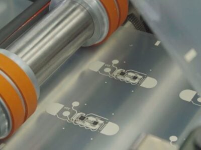
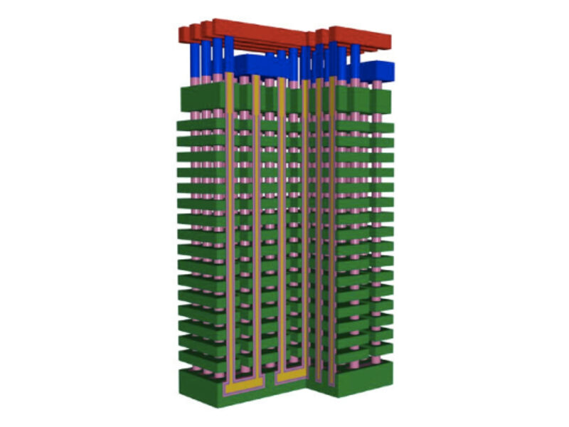
The Kioxia design features advanced architecture beyond the conventional eight-stagger memory hole array and achieves up to 10 percent greater lateral cell array density compared to the fifth-generation technology.
This 3D-NAND lateral scaling advancement, in combination with 162 layers of stacked vertical memory, enables a 40 percent reduction in die size compared to the previous generation 112-layer stacking technology. As with all other flash memory suppliers the competition has moved to the vertical dimension with flash memories inability to scale much below 40nm node in the planar dimensions. Kioxia and Western Digital produce nearly a third of the world’s memories, but missed out on joining SK Hynix and Micron in the 176-layer 3D-NAND club.
However, Kioxia and Western Digital argue that if you can achieve the same bit density in fewer layers you will likely improve yield.
“With this new generation, Kioxi and Western Digital are introducing innovations in vertical as well as lateral scaling to achieve greater capacity in a smaller die with fewer layers. This innovation ultimately delivers the performance, reliability and cost that customers need,” said Siva Sivaram, President of Technology & Strategy, Western Digital, in a statement issued by Kioxia.
The Kioxia and Western Digital teams also applied Circuit Under Array CMOS placement and four-plane operation, which together deliver nearly 2.4 times improvement in program performance and 10 percent improvement in read latency compared to the previous generation. I/O performance also improves by 66 percent, enabling the next-generation interface to support the ever-increasing need for faster transfer rates.
Overall, the new 3D-NAND flash memory technology reduces the cost per bit, as well as increases the manufactured bits per wafer by 70 percent, compared with the previous generation.
www.kioxia.com; www.westerndigital.com
Related 3D-NAND articles:
- 3nm GAA process, compute-in-memory among highlights of ISSCC 2021
- SK Hynix joins Micron on 176 layers
- Kioxia announces another NAND wafer fab
Other articles on eeNews Europe
- Europe needs to wake from its 30-year semiconductor sleep
- Battle for the AI toolflow
- UK to launch £800m research agency
- Mars helicopter readies for takeoff
- Bosch in blockchain trial for secure AIoT
 If you enjoyed this article, you will like the following ones: don't miss them by subscribing to :