European research takes lead in pushing transistor design
Researchers from IMEC (Leuven, Belgium) have shown the feasibility of a buried power rail (BPR) for use with a FinFET architecture for CMOS scaling beyond 5nm. The is a part of the Forksheet transistor concept previously laid out by IMEC (see Here comes the forksheet transistor, says IMEC).
Forksheet transistors are not due to be presented at VLSI Symposia on Technology and Circuits, which has gone virtual for 2020 and takes place June 15 to 19. But the IMEC paper demonstrates the integration of the tungsten BPRs with silicon FinFETs and that the presence of floating BPRs does not have a deleterious effect on nearby CMOS transistors.
The paper also reports that a tungsten buried power rail BPR interfaced with ruthenium via contact can withstand more than 320 hours of electromigration stress at 4MA/square centimetre and 330 ºC. This makes ruthenium a candidate for via metallization for BPR.
Paper T-HL-6 “Buried Power Rail Integration with Si FinFETs for CMOS Scaling beyond the 5nm Node” by Anshul Gupta et al., IMEC.

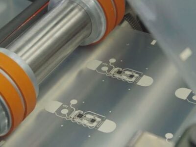
Cross section showing buried power rail within FinFET process. Source: IMEC, VLSI Symposium on Technology
In the middle of the last decade IMEC was a pioneer of the evolution of FinFETs to gate-all-around (GAA) transistors as nanowire and nanosheet transistors. It gained interest from Samsung and Globalfoundries although the latter has dropped out of leading-edge semiconductor manufacturing.
At the VLSI Symposia CEA-Leti (Grenoble, France) researchers are due to report on extending the nanosheet transistor to seven layers. Leti has made these transistors and observed higher performance due to the higher effective channel width (Weff) as compared to the state of the art FinFET transistors.
The researchers at Leti evaluate the trade-off of increasing the footprint to achieve greater Weff to boost device performance with process complexity.
They demonstrate, for the first time, seven-level stacked GAA nanosheet transistors fabricated using a replacement metal gate process, inner spacer, and self-aligned contacts. They demonstrate excellent gate controllability with extremely high current drivability threefold increase in drain current over usual two-level stacked NS GAA transistors.
Paper T-C1-2 “7-Level-Stacked Nanosheet GAA Transistors for High Performance Computing” Sylvain Barraud et al., CEA-LETI-MINATEC.
Related links and articles:
News articles:
Forksheet transistor enables 2nm chip node
Here comes the forksheet transistor, says IMEC
IMEC presents ‘n-over-p’ complementary FET proposal
Sony, Kioxia pursue ferroelectric non-volatile memory
 If you enjoyed this article, you will like the following ones: don't miss them by subscribing to :